Technical / Research - Page 15

Micron and A*STAR to jointly develop high density STT-MRAM

Micron and the A*STAR Data Storage Institute (DSI) from Singapore announced that they will jointly develop STT-RAM. The two companies will invest in a 3-year joint-research program to develop high-density STT-MRAM devices.

Years ago Micron had an active MRAM program which was scrapped in October 2004. It's great to see them re-enter MRAM research. Scott DeBoer, Micron Vice President of Research and Development said that Micron is "actively working on multiple emerging memory development programs" - and this collaboration is seen as a way to "explore the potential of STT-MRAM"

Read the full story Posted: Oct 29,2011

MRAM for Biomolecules concept developed using microfluidics and magnetic switches

Researchers from the National Institute of Standards and Technology (NIST) and University of Colorado Boulder (CU) developed a new chip that uses microfluidics and magnetic switches to trap and transport magnetic beads. This low-power device may be useful for medical devices. This technology may also lead us towards "MRAM" chips used for molecular and cellular manipulation.

In the past, magnetic particle transport chips required continuous power and even cooling. This new technology manages to overcome the power and heat issues, and offers random-access two-dimensional control and non-volatile memory. The prototype chip uses 12 spin valves (commonly used as magnetic sensors in HD read heads) which are optimized for magnetic trapping. Pulses of electric current are used to switch individual spin valve magnets “on” to trap a bead, or “off” to release it, and thereby move the bead down a ladder formed by the two lines. The beads start out suspended in salt water above the valves before being trapped in the array.

Read the full story Posted: Oct 22,2011

HP and Hynix to launch flash-replacement Memristor products in 2013

HP says that their two terminal memristor (Resistive RAM) technology will be launched in 18 months - and will "start to take market share from flash memory". The company has 'big plans' for the new memory technology and are working with Hynix to launch the flash replacement chip in 2013. The company also plans to go after the DRAM market in 2014/2015 and later the SRAM market as well.

HP has over 500 patents on this technology alone - but it isn't the only company working on memristor devices - in fact Samsung has an even bigger team working on a similar project.

Read the full story Posted: Oct 09,2011

Rare earth atoms on graphene may be useful for MRAM

Researchers from the US Ames Laboratory discovered that rare-earth minerals dysprosium and gadolinium react strongly with graphene, while lead does not. They say that the RE minerals act like tiny magnets on Graphene - and are quite good magnets. This could lead to applications in MRAM, for example. 

Rare earth minerals on graphene

Read the full story Posted: Oct 04,2011

Toshiba to use MRAM as cache for HDD and NAND

Kiyoshi Kobayashi, president of Toshiba's Semiconductor and Storage Products Company, said that "MRAMs will make it possible to take further advantage of NAND flash memories and HDDs, whose access performances are low,". It seems that Toshiba plans to use MRAM as cache for both NAND and HDDs devices.

Toshiba hasn't given up on the idea of having a full MRAM memory device - replacing HDD/NAND/DRAM altogether, but using it as a cache can be a step towards this goal.

Read the full story Posted: Aug 17,2011

Toshiba and Hynix to co-develop and produce MRAM products

Toshiba and Hynix announced an agreement to jointly develop MRAM products. Once the development is complete, the companies intend to establish an MRAM production plant together. We believe the companies intend to develop STT-MRAM technology.

Toshiba has been developing STT-MRAM for quite some time, and just a few days ago reported a breakthrough MTJ device that could pave the way towards Gigabit MRAM devices. They expect such chips within 3-4 years, so that's probably the same time frame on the new JV with Hynix.

Read the full story Posted: Jul 13,2011

Toshiba report STT-MRAM advances, expects gigabit chips within 3-4 years, to be cost competitive to DRAM

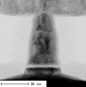
Toshiba says that their newly developed perpendicular magnetization-type magnetic tunnel junction (MTJ) device has excellent properties - and it can be a basic element towards a gigabit STT-MRAM device. The company says that these 'research results' are encouraging and they will now shift to the development of products. Commercialization of gigabit STT-MRAM is expected within 3 to 4 years.

MTJ cross section (Toshiba)MTJ cross section (Toshiba)

The device's writing current density is 5 x 10⁵Acm-2, which is 1/6 that of the company's existing products. And its magnetic resistance (MR), which determines data reading margin, is 200%, which was drastically improved from the 15% of the existing products. Toshiba managed to have both a low writing current density and a high MR ratio by using cobalt and iron based materials for the recording layer.

Read the full story Posted: Jul 06,2011

Spingate invented a spin-based nonvolatile FPGA

Spingate invented a nonvolatile field-programmable gate array (FPGA) technology employing the company's proprietary spin logic. The spin logic represents an elegant synthesis of conventional CMOS logic with embedded magnetic tunnel junctions (MTJs) residing above the silicon. The embedded MTJs use a spin induced writing mechanism to reverse a magnetization in a storage magnetic layer. The proper use of these MTJs enable the entire circuit to be non-volatile.

The company has several pending patents that cover basic components of the new technology: logic gates, latches, flip-flops, adders, multiplexers, etc. According to Spingate, the nonvolatile FPGA technology has an excellent scalability and almost zero power consumption in a standby mode of operation. It can provide a significant reduction of interconnects and chip size. The new technology can effectively compete with existing FPGA technologies in price and performance.

Read the full story Posted: Jul 02,2011

Crocus developed NAND-like MRAM based technology called Magnetic Logic Unit (MLU)

Crocus developed a new technology called Magnetic-Logic-Unit (MLU), which is an evolution of their Thermally Assisted Switching (TAS) technology. MLU allows for practical implementation of advanced logic and memory capabilities - which will enable new applications in high density data storage, secure commerce and communications, high performance network processing and high temperature automotive and industrial markets.

Crocus' MLU provides stability to the stored data in normal operation. The MLU's reference leayer can be configured in three ways:

  • With Fixed magnetization to implement a traditional NOR function
  • With floating magnetization to implement a NAND function
  • With driven magnetization to implement an XOR function, which ultra-secure compare and encrypt function.
Read the full story Posted: Jun 22,2011

NEC and Tohoku University developed MRAM based spin-CAM

NEC Corporation and Tohoku University have developed an MRAM based CAM (content addressable memory) that includes non-volatile storage by using the vertical magnetization of vertical domain wall elements in a cobalt-nickel active layer. They call this Spin-CAM.

NEC and Tohoku built a 16-kbit Spin-CAM prototype chip (using a 90-nm process). This chip features 5 ns search cycle time, 200-microamps write current and a 6.6 square micron memory cell. Such a CAM may be used to create instant-on electronics and zero-electricity standby modes.

Read the full story Posted: Jun 13,2011