Toshiba says that their newly developed perpendicular magnetization-type magnetic tunnel junction (MTJ) device has excellent properties - and it can be a basic element towards a gigabit STT-MRAM device. The company says that these 'research results' are encouraging and they will now shift to the development of products. Commercialization of gigabit STT-MRAM is expected within 3 to 4 years.
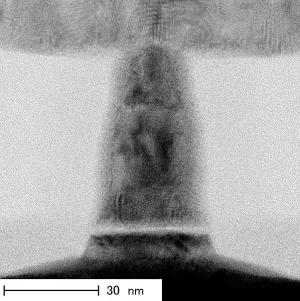
 MTJ cross section (Toshiba)
The device's writing current density is 5 x 10⁵Acm-2, which is 1/6 that of the company's existing products. And its magnetic resistance (MR), which determines data reading margin, is 200%, which was drastically improved from the 15% of the existing products. Toshiba managed to have both a low writing current density and a high MR ratio by using cobalt and iron based materials for the recording layer.
Toshiba says that they have made an MTJ device in a 30nm process, and that it works properly. And the process size and cell area of the new MTJ device can be further reduced, according to the company - they aim at a process size one generation older than that of DRAM and a cell area of 6F2. Production cost will be the same as DRAM (in theory, anyway).
Toshiba has been researching MRAM since 2004, and in 2007 the company fabricated their first STT-MRAM cell. In 2008, the company reported advances in this research and said that they expect MRAM to 'take over DRAM in 2015'. It seems that their time frames are the same ( the current prediction of mass production is 3-4 years, or 2014-2015).

