Renesas Electronics announced that it has developed circuit technologies for embedded STT-MRAM that reduces the energy and voltage of the memory write operation.
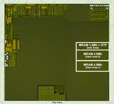
Renesas produced a 22-nm MCU test chip, that includes a 10.8 Mbit embedded MRAM memory cell array. It achieves a random read access frequency of over 200 MHz and a write throughput of 10.4-megabytes-per-second (MB/s).
Renesas says that it developed two specific new circuit technologies, one for faster MRAM read operations and one for faster write operations. Renesas says that it can achieve the world's fasterst random access speed of 4.2 ns.
To increase read operation speed, Renesas introduced two mechanisms. The first mechanism aligns the reference current in the center of the window according to the actual current distribution of the memory cells for each chip measured during the test process. The other mechanism reduces the offset of the sense amplifier.
To increase write operation speed, Renesas took into account that because the power supply conditions used in test processes and by end product manufacturers are stable, the lower voltage limit of the external voltage can be relaxed. Thus, by setting the higher step-down voltage from the external voltage to be applied to all bits in the first phase, write throughput can be improved 1.8-fold.
These new technologies follow on Renesas' previous MRAM work. In 2021, the company announced that it has developed two technologies that reduce the power consumption of STT-MRAM chips by 72%. In 2022, Renesas announced that it has developed 22-nm embedded STT-MRAM circuit technologies.


