Veeco Nexus Ion-Beam deposition system ad
Veeco produced a nice ad showing their NEXUS Ion Beam Deposition System. This tool is "ideal for MRAM applications" and can also be used for read/write heads used in hard disk drives:
Veeco produced a nice ad showing their NEXUS Ion Beam Deposition System. This tool is "ideal for MRAM applications" and can also be used for read/write heads used in hard disk drives:
 There are reports that Toshiba decided not to bid in the corporate rehabilitation efforts of Elpida Memory. But Toshiba does plan to offer a joint MRAM project to whoever takes over Elpida's DRAM factory in Japan. Toshiba is already collaborating with Hynix on MRAM.
It is expected that two companies will bid (this is the second round of bidding) - Micron Technology (who are developing STT-MRAM together with A*STAR) and a joint bid by the US investment fund TPG Capital and a fund under the Lenovo Group.
A*STAR scientists have filed a patent on low-density parity-check (LDPC) coding with soft decision decoding. This is an advanced error correction coding scheme STT-MRAM devices. Hopefully this new scheme will enable more relaxed smaler STT-MRAM designs that can rely on the error-correction.
STT-MRAM devices suffer from cell errors due to imperfections in the fabrication process (variation in the tunneling oxide thickness and cross-section area). The researchers explain that conventional (hard decision) error correction codes do not work very well on STT-MRAM cells. The new soft decision decoding works on the probability of each detected bit as being a 0 or 1 (i.e. soft reliability), and hence has less decoding errors than the conventional hard decision decoding.
Researchers at the Max Planck Institute of Microstructure Physics in Halle developed a new switching mechanism for magnetic current. The new mechanism could be used to store information in four states of a storage point, not just two - which doubles storage density or lowers the size of MRAM devices. It may also have other implications for Spintronic Devices. The idea is to use a short electric pulse to change the magnetic transport properties of a material sandwich consisting of a ferroelectric layer between two ferromagnetic materials.

In ferroelectric materials, voltage switches between the two directions of an electric polarisation depending on its polarity not unlike when a magnetic field permanently reverses the polarity of a ferromagnet. As ions shift within the material structure during this process, the polarisation remains intact, even after the voltage has been reduced. It is possible, however, to reverse the switch again with a similarly large voltage with reversed polarity.
 Crocus is a startup company that develops MRAM technology - and recently they have announced several exciting advances in both their technology and their financing and production plans. We had the good chance to interview Barry Hoberman, Crocus' chief marketing officer.
Q: Barry, thanks for agreeing to answer our questions... The big story today is still RUSNANO's $125 million investment - announced in May 2011. Any updates on this deal? Have the construction begun on the Russian plant?
A: The site selection for our Russian plant (Crocus Nano Electronics) has been completed. The site contains an existing shell, which will be modified to support the clean room. Crocus expects to process wafers at this facility in 2013.
 Crocus signed a technology development and wafer manufacturing agreement with China's Semiconductor Manufacturing International Corp. (SMIC). The two companies will develop high-temperature Magnetic Logic Unit (MLU) technology targeted at automotive applications. The base wafer processing will be done by SMIC and these wafers will be further processed by Crocus at a facility that has yet to be built in Russia.
In addition the MLU technology could be licensed to SMIC for use in embedded chip applications and the two companies plan to market jointly smart cards made using TAS MLU and MRAM technology.
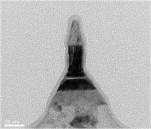
Samsung developed a perpendicular MTJ element using 17nm technology - the world's smallest. This paves the way towards sub-20nm STT-MRAM. Up until now it was believed that to create such a small P-MTJ you will have to use a multi-layer structure and a rare-earth material for the ferromagnetic electrode. Samsung however used regular materials and structure (Ta/CoFeB/MgO/Ta) and optimized the oxidation process for the tunnel insulator (MgO).

By increasing the anisotropic energy on the joint interface the perpendicular magnetization of the ferromagnetic electrode was stabilized. Samsung reports a thermal stability factor of 34, a TMR ratio of 70% and a writing current of 44microampere with a perpendicular magnetization MTJ element whose cross-section area is 17 x 40nm. There is still room for improvement in the thermal stability factor in order to achieve over 1Gbit capacity at 20nm. This can be realized by making more improvements to the newly developed oxidation process for the tunnel insulator

 Crocus announced that Morpho plans to develop smartcards based on Crocus' Magnetic-Logic-Unit (MLU) technology. The two companies signed an agreement under which Crocus will develop an MLU-based secure microcontroller which Morpho will integrate into its smart card products. The secure microcontroller product will be compliant with the latest quality and security standards.
According to Crocus, MLU technology (which is an adaption of thermally-assisted magnetic switching, or TAS, for use in memory access in addition to storage) offers the advantage of much higher read-write cycle endurance, compared with leading-edge flash memory, while also offering inherent non-volatility and low power operation. The use of MLU should also provide match-in-place capability, which can be used for secure authentication.
Toshiba has a new hybrid cache design that uses STT-MRAM and SRAM combination. This is aimed towards next-generation low-power computer processors. These new computers will usually be off, and the time and power it takes to "wake up" is considerable. The new design can reduce the energy consumption by around half - and does not effect processing capacity.

Toshiba's design uses a 512Kb STT-MRAM cache combined with a 32Kb register file and a 64Kb SRAM primary cache. Using the non-volatile MRAM, the power gating can be conducted more frequently. In current designs, it takes around 20 micro seconds to recover from power gating and about 150 micro seconds from deep-sleep mode. In the new design, it takes only 1 micro second to recover from power gating.
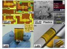
Researchers from the Korea Advanced Institute of Science and Technology (KAIST) developed new flexible non-volatile resistive random access memory (RRAM) on plastic. The team used memristors integrated with high-performance single-crystal silicon transistors.

This is the first time such a flexible memory is achieved. Bending memory cells causes cell-to-cell interference. To solve this problem, you have to integrate transistors. But most transistors built on plastic substrates (organic/oxide transistors) are not capable of achieving the sufficient performance level with which to drive conventional memory. The new single-crystal silicon transistors used by KAIST solve this issue.