Tohoku University

PSMC collaborates with Power Spin for MRAM production by 2029

Reports in Japan suggest that Taiwan's Powerchip Semiconductor Manufacturing (PSMC) will enter into a new MRAM R&D project, together with Japan's Power Spin. PSMC plans to start producing MRAM chips by 2029, at its 12-inch factory that it is now building in Japan.

Power Spin, that holds MRAM IP originally developed at Tohoku University, will license its IP to PSMC and will assist in the required R&D and ramp-up of production at PSMC's fab. PSMC looks to utilize the MRAM technology mainly for generative AI data center solutions.

Read the full story Posted: Feb 07,2024

Tohoku University researchers develop a high performance X nm MTJ

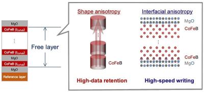
Researchers from Japan's Tohoku University developed a method to produce X nm MTJs, using a CoFeB/MgO stack structure. The researchers report that the extremely small device achieves both high-retention and high-speed. This was enabled by controlling the shape and interfacial anisotropies individually by varying the thickness of each CoFeB layer and the quantity of [CoFeB/MgO] stacks.

The researcher further report that shape anisotropy-enhanced MTJs showed good retention (> 10 years) at 150 °C at single nanometer sizes, whereas interfacial anisotropy-enhanced MTJs exhibited rapid speed switching (10 ns or less) below 1 V.

Read the full story Posted: Jan 19,2024 - 1 comment

Researchers from Tohoku University developed the world's smallest STT-MRAM MTJ

Researchers from Tohoku University managed to fabricate the world's smallest STT-MRAM MTJ, at 2 nm. In addition, the researchers demonstrated fast switching (3.5 ns) in sub-five-nm STT-MRAM MTJs.

10-nm MTJ TEM photo, Tohoku University

The new MTJ were developed using a new multilayered ferromagnetic structure that can engineer characteristic relaxation time, which governs the magnetization dynamics in the ns regime.

Read the full story Posted: Dec 14,2021

Researchers develop the world's smallest high-performance MTJ

Researchers from Tohoku University say they have developed the world's smallest (2.3 nm) high-performance magnetic tunnel junctions (MTJs).

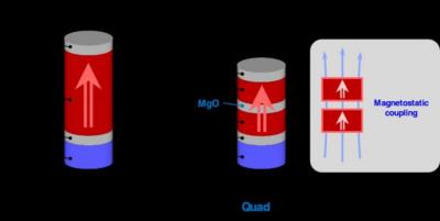
Shape anisotropy MTJ scheme (Tohoku University)

The design is based on the Shape-anisotropy MTJ (developed by the same researchers in 2018) in which thermal stability is enhanced by making the ferromagnetic layer thick. In this new research, the scientists used a new structure that uses magnetostatically coupled multilayered ferromagnets - which enabled the scaling down to 2.3 nm diameters.

Read the full story Posted: Dec 09,2020

Researchers in Japan developed a high-speed SOT-MRAM memory cell compatible with 300mm Si CMOS technology

Researchers at Tohoku University demonstrated a high-speed spin-orbit-torque MRAM (SOT-MRAM) memory cell compatible with 300 mm Si CMOS technology.

The SOT device achieved high-speed switching (down to 0.35 ns) and a high thermal stability factor (E/kBT 70) which the researchers say is sufficient for high speed non-volatile memory applications. The device can withstand annealing at 400°C. The researchers used these devices to create a complete SOT-MRAM memory cell.

Read the full story Posted: Dec 10,2019

Tohoku University researchers develop the world's fastest STT-MRAM

Researchers from Japan's Tohoku University developed a 128 Mb STT-MRAM device that features a write speed of 14 nm, the world's fastest STT-MRAM chip at a density over 100 Mb.

Tohoku 128 MB STT-MRAM 14 ns write speed image

To achieve this high speed, the researchers developed MTJs that are integrated with CMOS, which also significantly reduces the power-consumption of the memory device.

Read the full story Posted: Dec 30,2018

Tohoku University develops ultra-small (<10nm) MTJs

Researchers from Tohoku University developed new ultra-small (single-digit nanometer scale) magnetic tunnel junctions (MTJs) that have sufficient retention properties and yet can be switched by a current.

Shape anisotropy and interfacial anisotropy MTJs (Tohoku University)

Tohoku University developed 20-nm CoFeB/MgO-based MTJs in 2010, in which an "interfacial anisotropy" at the CoFeB/MgO interface was utilized. But these will not work at under 20-nm. The researchers now used a "shape anisotropy" to achieve the smaller MTJs.

Read the full story Posted: Feb 22,2018

Keysight Technology announces a new MRAM test platform designed in collaboration with Tohoku University

Tohoku University's Center for Innovative Integrated Electronic System (CIES) announced that its collaboration with Keysight Technology has led to the release of a new MRAM test platform product, the NX5730A.

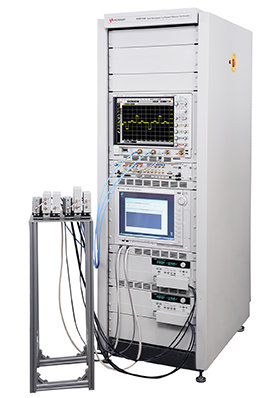
Kesight NX5730A Memory Test system photo

Keysight's NX5730A is a high-throughput 1 ns Pulsed IV memory test solution. Keysight says that this solution is a unique dedicated system for characterizing emerging devices such as magnetic tunnel junction (MTJ) on silicon wafers, accelerating the efficiency of device characterization and memory production testing.

Read the full story Posted: Nov 08,2017

Researchers develop a way to increase STT-MRAM density by placing MTJs directly on the via

Researchers from Japan's Tohoku University developed a technology to stack magnetic tunnel junctions (MTJs) directly on the the vertical interconnect access (via) without causing deterioration to its electric/magnetic characteristics. The researchers say that this technique can reduce the chip area of STT-MRAM.

Tohoku on-via STT-MRAM cell

The via in an integrated circuit design is a small opening that allows a conductive connection between the different layers of a semiconductor device. Placing the MTJ directly on the via holes has been avoided because it can degrade the MTJ's characteristics because the MTJ is very sensitive to the quality of the surface of its lower electrode.

Read the full story Posted: May 17,2016

Researchers suggest and demonstrate a new scheme of spin-orbit-torque (SOT) induced magnetization switching

Researchers at Tohoku University developed a new scheme of spin-orbit-torque (SOT) induced magnetization switching. In the new scheme the magnetization directed collinear with the current.

Structures of spin orbit torque induced magnetization

The researcher fabricated three-terminal devices with the new structure (using a Ta/CoFeB/MgO-based magnetic tunnel junction) and successfully demonstrated the switching operation. The research report a "reasonably small" required current density to induce the magnetization switching and a "reasonably large" resistance difference between 0 and 1 states. They say that this is a promising candidate for future MRAM devices.

 
Read the full story Posted: Mar 22,2016