 Intel is the world largest chip maker, and also manufactures networking, memory and communications products.
Intel is researching several next-generation memory technologies including MRAM memory. Over the years it has demonstrated several MRAM technologies.
2200 Mission College Blvd
Santa Clara, CA 95054-1537
United States
Taiwan's Semiconductor Research Institute developed an SOT-MRAM device based on a PMA technique
Researchers at Taiwan's Semiconductor Research Institute (TSRI) unveiled a new SOT-MRAM memory device that they developed in collaboration with University scientists.

The new device uses a perpendicular magnetic anisotropy (PMA) technique. According to the TSRI researchers, they are the second team to successfully produce MRAM chips based on PMA (Intel is the first team to have achieved this).
Intel researchers demonstrate 2MB STT-MRAM arrays suitable for on-chip L4 cache applications
Intel researchers have demonstrated 2MB STT-MRAM devices that are suitable for on-chip L4 cache applications. Intel says these devices feature data retention, endurance and bit error rates good enough for L4 cache.

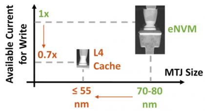
Intel's new STT-MRAM features 20 nm write times, 4 ns read times, an endurance of 1012 cycles and memory retention of one second at 110 degrees. The bit rates are good enough to be handled with error-correcting code (ECC) techniques. To achieve these features, Intel reduced the magnetic junction size to 55 nm (from 70-80 nm it had achieved before).
Intel says its embedded 22nm MRAM is production ready
In October 2018 Intel revealed that it is developing embedded MRAM - and that the company has successfully integrated embedded MRAM into its 22nm FinFET CMOS technology on full 300mm wafers.
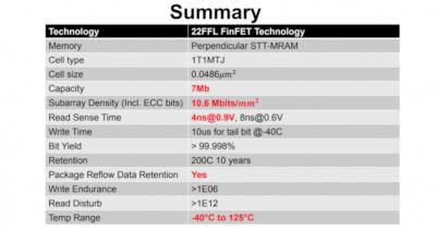
Now Intel gave more details on its embedded STT-MRAM, and said that the technology is ready for high-volume manufacturing. Intel said it has used a "write-verify-write" scheme and a two-stage current sensing technique to create 7Mb perpendicular STT-MRAM arrays in its 22FFL FinFET process.
Intel is developing embedded MRAM technologies
Intel says it will present a new paper detailing its MRAM research at the International Electron Devices Meeting (IEDM) in early December 2018. This is the first time we hear of any MRAM R&D at Intel which is great news, even if it just a research paper.

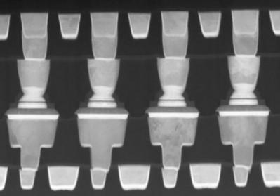
Intel has apparently successfully integrated embedded MRAM into the company's 22nm FinFET CMOS technology on full 300mm wafers. The magnetic tunnel junction-based memory cells are built from dual MgO magnetic tunnel junctions (MTJs) separated by a CoFeB-based layer in a 1 transistor-1 resistor (1T-1R) configuration in the interconnect stack. Intel has manufactured a 7.2Mbit array with reported data retention figures in excess of 10 years and write endurance of greater than 10^6 cycles.
Intel and Numonyx announced a new higher-density phase change memory technology
Intel and Numonyx have announced a new memory technology that "paves the way for scalable, higher density phase change memory (PCM) products". They have created a 64Mb chip that enables to stack multiple layers of PCM arrays in a single die. They cal it PCMS (phase change memory and switch).
Intel Says PRAM Volume Production to Start in 2H of 2007
 Intel Corp. has revealed a prototype PRAM (phase change RAM) wafer, long under development, at IDF Spring 2007 in Beijing, China, which began on April 16, 2007. At the keynote speech, Intel's CTO Justin Rattner announced, "the company will start mass-production of PRAM as early as the second half of 2007." He also said, "We consider replacing NOR flash memory with PRAM first, but that's not our goal. PRAM may possibly replace DRAM in the near future. We are paying a lot of attention to the technology."
Intel set for first public demo of PRAM
 Intel's chief technology officer Justin Rattner is set to give the first public demonstration of the company's PRAM (phase-change RAM) technology at this week's Intel Developer Forum (IDF) conference.
PRAM is based on chalcogenide glass, which can be altered using the heat generated by an electric current. Heat changes the physical structure of the glass to either a crystalline or amorphous state. Each of these states has a distinct electrical resistance that is used to represent the ones and zeroes needed to represent stored data in binary terms.
Intel to sample PRAM this year
 Intel's new phase-change memory technology, called PRAM by Intel and PCM by others who are working on the same type of memory, is set to sample in the first half of this year. Intel says they plan to ship the first PRAM modules as a straight-ahead NOR flash replacement so that they can work the kinks out of the design before trying to move it up the memory hierarchy. The company claims a much higher number of read-write cycles (100 million) than flash, as well as a potential 10 years' worth of data retention.


