STT-MRAM: Introduction and market status - Page 5
Successful MRAM Production Requires Good Magnetic Test Equipment
This is a sponsored post by Integral Solutions Int'l
MRAM is likely to be the most promising next-generation non-volatile memory technology today. Toggle MRAM and STT-MRAM are already entering the market, gaining market share in many applications. Next-generation MRAM technologies, such as SOT-MRAM could enable the replacement of even the fastest SRAM applications, with higher densities.
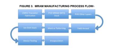 Source: Coughlin Associates, 2019
The MRAM production process has many stages, as device architecture is relatively complex, with a magnetic cell (frontplane) fabricated on top of a CMOS backplane. (use Figure 2 or Figure 3 from Coughlin). Measurement and characterization of devices are highly important, and the production of MRAM memories depend on measurement tools are are specialized for MRAM and STT-MRAM measurements.
Everspin reports its Q4 2019 financial results
Everspin Technologies announced its Q4 2019 financial results, with revenues of $9.8 million (up 5% from Q3 2019) and a net loss of $3.1 million, down from a net loss of $3.7 million in Q3 2019.
In 2019, Everspin reports revenues of $37.5 million and a net loss of $14.7 million, down from $17.8 million in 2018.
Everspin and Globalfoundries extend their MRAM agreement to 12 nm processes
Everspin Technologies announced that it has amended its STT-MRAM joint development agreement (JDA) with GLOBALFOUNDRIES to set the terms for a future project on an advanced 12 nm FinFET MRAM solution. Everspin agreement included 40 nm, 28 nm and 22 nm processes, and now also include 12 nm.
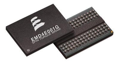
GF recently announced it has achieved initial production of embedded MRAM (eMRAM) on its 22FDX platform.
Researchers show how antiferromagnetic STT-MRAM technology can enable higher-density and lower energy memory
Researchers from Northwestern University suggest building STT-MRAM devices from antiferromagnetic materials - as opposed to the currently-used ferromagnetic ones. The researchers say that these materials will enable higher-density devices that feature high speed writing with low currents.
Antiferromagnetic materials are magnetically ordered at the microscopic scale, but not at the macroscopic scale. This means that there is no magnetic force between adjacent bits in MRAM cells built from these materials - which means you can pack them very close together.
New super-lattice SL-STT-MRAM enable faster and more efficient memory architecture
Researchers from the National Taiwan University developed a new ultra low power STT-MRAM architecture, called Super Lattice STT-MRAM, or SL-STT-MRAM. The researchers say that SL-STT-MARM simultaneously achieves ultra-high MR ratio, high-speed switching, and low RA.

An SL-STT-MRAM is based on an SL-STT-MTJ, which uses a superlattice barrier to replace the single crystalline (MgO) barrier in traditional STT-MTJ. The superlattice barrier is made of alternating metal and insulator layers, in which only amorphous rather than single crystalline is used in the insulator. The SL-STT-MRAM features higher reliability for repeated writing than compared to traditional MgO based STT-MRAM.
Everspin starts production shipments of its 1Gb STT-MRAM chips
Everspin Technologies announced that It is has received the qualification notice from a major OEM for its 1Gb STT-MRAM device. The company is now qualified to start making production shipments of its new chip for its first customer.

Everspin further announced that since it started MRAM production, it shipped over 120 Toggle MRAM and STT-MRAM devices.
Intel researchers demonstrate 2MB STT-MRAM arrays suitable for on-chip L4 cache applications
Intel researchers have demonstrated 2MB STT-MRAM devices that are suitable for on-chip L4 cache applications. Intel says these devices feature data retention, endurance and bit error rates good enough for L4 cache.
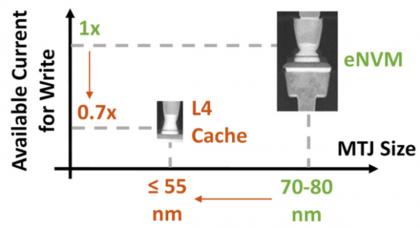
Intel's new STT-MRAM features 20 nm write times, 4 ns read times, an endurance of 1012 cycles and memory retention of one second at 110 degrees. The bit rates are good enough to be handled with error-correcting code (ECC) techniques. To achieve these features, Intel reduced the magnetic junction size to 55 nm (from 70-80 nm it had achieved before).
Everspin announces its Q3 2019 financial results
Everspin Technologies announced its financial results for Q3 2019 - with revenues of $9.2 million (down from $11.5 million in Q3 2018) and a net loss of $3.7 million (down from $5.6 million in Q3 2018). Everspin says that it achieved record STT-MRAM revenues.

At the end of the quarter, Everspin had $14.8 million in cash and equivalents. For the next quarter, it expects revenues to be between $9.3 million and $9.7 million.
IBM to use Everspin's 1Gb STT-MRAM in its next-gen FlashCore modules
In August 2018 IBM announced that it adopted Everspin's 256Mb STT-MRAM chips in its enterprise SSD FlashSystem. Now IBM announced that it's latest FlashCore modules will use Everspins 1Gb STT-MRAM chips.

Using MRAM instead of DRAM memory enabled IBM to remove the relatively large supercapacitors (used to make the DRAM non-volatile) and so the company was able to reduced the size of its drives and switch to a standard 2.5-inch U.2 drive form factor.
Cadence to offer design and verification support for Everspin's 1Gb STT-MRAM
Everspin Technologies announced that Cadence Design is now providing DDR4 Design IP (DIP) and Verification IP (VIP) support for Everspinâs 1 Gb STT-MRAM memory. Cadence has supported Everspin's STT-MRAM products since 2012. Everspin customers will now be able to request 1Gb MRAM-enabled IP and VIP for their Custom ASIC solutions.

Everspinâs 1 Gb STT-MRAM product family includes both 8bit and 16-bit DDR4 compatible (ST-DDR4) interface versions of the device and are available in a JEDEC-compliant BGA package.
Pagination
- Previous page
- Page 5
- Next page


