Toshiba report STT-MRAM advances, expects gigabit chips within 3-4 years, to be cost competitive to DRAM
Toshiba says that their newly developed perpendicular magnetization-type magnetic tunnel junction (MTJ) device has excellent properties - and it can be a basic element towards a gigabit STT-MRAM device. The company says that these 'research results' are encouraging and they will now shift to the development of products. Commercialization of gigabit STT-MRAM is expected within 3 to 4 years.
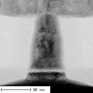
 MTJ cross section (Toshiba)
The device's writing current density is 5 x 10⁵Acm-2, which is 1/6 that of the company's existing products. And its magnetic resistance (MR), which determines data reading margin, is 200%, which was drastically improved from the 15% of the existing products. Toshiba managed to have both a low writing current density and a high MR ratio by using cobalt and iron based materials for the recording layer.
Toshiba - advances in 1Gb MRAM. Expects MRAM to take over DRAM in 2015
Toshiba is still working on 1Gb MRAM chips, and it's "almost ready". They are using Spin-RAM (STT-RAM), like IBM.
Toshiba's projections sees MRAM taking over DRAM in 2015.
Toshiba develops new MRAM device which opens the way to giga-bits capacity
Toshiba Corporation today announced important breakthroughs in key technologies for MRAM. The company has successfully fabricated a MRAM memory cell integrating the new technologies and verified its stable performance.
In making these major advances, Toshiba applied and proved the spin transfer switching and perpendicular magnetic anisotropy (PMA) technologies in a magnetic tunnel junction, which is a key component in the memory cell.
Spin transfer switching uses the properties of electron spin to invert magnetization and writes data at very low power levels. It is widely regarded as a major candidate among next-generation principles for new memory devices. PMA aligns magnetization in the magnetic layer perpendicularly, either upward or downward, rather than horizontally as in in-plane shape anisotropy layers. The technology is being increasingly used to enhance for storage capacity for high-density hard disc drives (HDDs), and Toshiba has successfully applied it to a semiconductor memory device. With PMA data write operation and magnetic switching can be achieved at a low energy level. Toshiba also overcame the hurdle of achieving the required precision in the interface process and significantly cutting write power consumption.
In order to realize a miniature memory cell based on PMA, Toshiba optimized the materials and device structure of the new MRAM. Close observation of performance confirms stable operation (see the diagram for full explanation of structure). Toshiba will further enhance development toward establishing fundamental technologies within the coming years.
Development of the new MRAM technologies was partly supported by grants from Japan’s New Energy and Industrial Technology Development Organization (NEDO).
Toshiba and NEC Develop World's Fastest, Highest Density MRAM
Toshiba Corporation and NEC Corporation today announced that they have developed a magnetoresistive random access memory (MRAM) that combines the highest density with the fastest read and write speed yet achieved. The new MRAM achieves a 16-megabit density and a read and write speed of 200-megabytes a second, and also secures low voltage operation of 1.8V.
A major challenge of MRAM development to date has been the acceleration of read speeds: the current drive circuit used to generate the magnetic field for writing degrades read operation from memory cells. The new MRAM has an improved circuit design that divides the current paths for reading and writing, realizing a faster read speed. It also reduces equivalent resistance in wiring by approximately 38% by forking the write current. These innovations together achieve a read and write speed of 200-megabytes a second and a cycle time of 34 nanoseconds â both the world's best performance for MRAM. This performance is underlined by a low operating voltage of only 1.8V, the ideal voltage for mobile digital products.
Alongside advances in performance, the new MRAM achieves advances in chip size. Toshiba and NEC have introduced the above mentioned technologies and optimized overall circuit design, achieving a chip that, at 78.7mm2, is approximately 30% smaller than its equivalent without the new circuit design. The new MRAM is the world's smallest in the 16-megabit era.
TSMC, NEC, Toshiba describe novel MRAM cells
TSMC claims to have developed novel MRAM structures based on a 0.18-micron process and a pillar write word line (PWWL) cell. The company proposes to shrink the bit size by a "so-called ExtVia process" while reducing the writing current by a factor of two.
Toshiba and NEC jointly presented a paper on a low-power 6F2 MRAM based on a cross-point cell. The 1-megabit MRAM chip is said to have been manufactured in a 130-nm process and a 0.24 x 0.48-micron2 magnetic tunnel junction technology. The chip is said to have a 250-ns access time and 1.5-volt operations. "To suppress the sneak current, a cell design is proposed for the new (cross-point) cell with a hierarchical bit line architecture".
Pagination
- Previous page
- Page 2


