Technical / Research - Page 3

Renesas develops 22-nm circuit technologies for embedded STT-MRAM

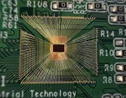
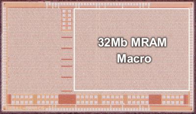
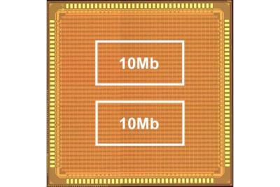
Renesas announced that it has developed 22-nm embedded STT-MRAM circuit technologies. Renesas developed a test 32-megabit (Mbit) chip with an embedded MRAM memory cell array that achieves 5.9-nanosecond (ns) random read access at a maximum junction temperature of 150°C, and a write throughput of 5.8-megabyte-per-second (MB/s).

To achieve this performance, Renesas developed two technologies. The first is a fast read technology employing high-precision sense amplifier circuit, utilizing capacitive coupling. The second is a fast write technology, with simultaneous write bit number optimization and shortened mode transition time.
Read the full story Posted: Jun 18,2022

Researchers demonstrate an ultra-fast and efficient laser-induced opto-MRAM device

Researchers from Eindhoven University of Technology (TU/e) and the Fert Beijing Institute of Beihang University have experimentally demonstrated a fully-functional picosecond opto-MRAM building block device, by integrating ultrafast photonics with spintronics.

The researchers used a femtosecond (fs) laser, which is the fastest stimuli commercially that enabled the device to be extremely fast - and also a thousand times more energy efficient compared to standard MRAM devices. The device is based on the femtosecond laser-induced all-optical switching (AOS) scheme in synthetic ferrimagnetic multilayers that was discovered by TU/e in 2017, integrating it with MRAM bit

Read the full story Posted: Apr 30,2022

ITRI and UCLA to co-develop VC-MRAM technologies

Taiwan-based Industrial Technology Research Institute (ITRI) announced an agreement with the University of California, Los Angeles (UCLA) to co-develop Voltage-Control MRAM (VC-MRAM) technologies.

UCLA-ITRI-VC-MRAM-prototype

ITRI says that VC-MRAM is a type of SOT-MRAM that offers improved performance - 50% higher writing speed and 75% less energy consumption. VC-MRAM is said to be ideal for AIoT and automotive industry applications. The partnership is expected to strengthen the link between both parties and accelerate the R&D and industrialization of new memory technologies.

Read the full story Posted: Mar 04,2022

NTU and TSMC researchers develop a new SOT-MRAM structure with high spin-orbital Hall conductivity

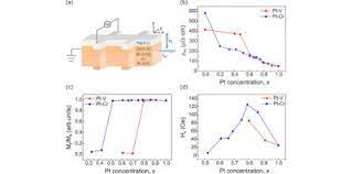
Researchers from National Taiwan University in collaboration with TSMC developed a new SOT-MRAM device structure, that features sizable orbital currents. This research promises a pathway for enhancing SOT-MRAM performance by harnessing both the conventional spin currents and the emergent orbital currents.

NTU TSMC PtCr Alloys SOT-MRAMThe new device is based on 3d light transition metals (such as V and Cr) that are incorporated into the classical spin Hall metal Pt. The Pt-Cr alloy enhances the charge-to-spin conversion efficiency which can realize high spin-orbital Hall conductivity, beyond the conventional spin Hall limit.
Read the full story Posted: Feb 27,2022

Researchers developed an ultra low power BiSb-based SOT MRAM device

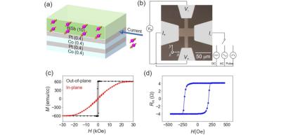
Researchers from the Tokyo Institute of Technology developed an ultrahigh-efficiency SOT magnetization switching in fully sputtered BiSb(Co/Pt) multilayers with large perpendicular magnetic anisotropy (PMA).

Scheme of ultra low power BiSb SOT-MRAM device (Tokyo IT)

The new device offers a large spin Hall angle and high electrical conductivity, thus satisfying all the three requirements for SOT-MRAM implementation. The researchers managed to achieve robust SOT magnetization at a low current density despite the large PMA field.

Read the full story Posted: Feb 23,2022

Samsung researchers are first to demonstrate MRAM-based in-memory computing

Researchers from Samsung's Advanced Institute of Technology (SAIT), have demonstrated what they say is the world’s first in-memory computing based on MRAM, targeting next-generation AI chips.

The researchers explain that In-Memory computing is a new paradigm that seeks to perform both data storage and data computing in a memory network. In such a computing system, a large amount of data, stored in the memory network, can be executed in a highly parallel manner. Power consumption in such systems is substantially reduced.

Read the full story Posted: Jan 13,2022

Researchers use MIFL to increase the magnetoresistance of pMTJs

Researchers from the University of Arizona developed a new pMTJ structure that exhibits high magnetoresistance, strong retention and is likely to achieve fast switching times as well.

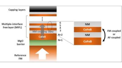
pMTJ with multi-interface free layer (Arizona University)

The new structure uses a multi-interface free layer (MIFL) which incorporate multiple materials with different properties. The researchers used a ferromagnetic CoFeB layer with nonmagnetic Mo or MgO layers. The magnetoresistance can be controlled by changing the thickness of the CoFeB layer. The researchers managed to demonstrate a magnetoresistance of over 200%.

Read the full story Posted: Dec 31,2021

Researchers from Tohoku University developed the world's smallest STT-MRAM MTJ

Researchers from Tohoku University managed to fabricate the world's smallest STT-MRAM MTJ, at 2 nm. In addition, the researchers demonstrated fast switching (3.5 ns) in sub-five-nm STT-MRAM MTJs.

10-nm MTJ TEM photo, Tohoku University

The new MTJ were developed using a new multilayered ferromagnetic structure that can engineer characteristic relaxation time, which governs the magnetization dynamics in the ns regime.

Read the full story Posted: Dec 14,2021

New SOT-MRAM device structure can be scaled up and is highly efficient

Researchers from Northwestern University, in collaboration with researchers from China, Italy and France, developed a new SOT-MRAM device structure that enables deterministic switching without any need for bias magnetic fields.

The new approach, unlike most earlier methods, can be scaled to large wafers with good uniformity, since it doesn't rely on having a structural asymmetry in the device. SOT-MRAM devices based on this structure could be faster and more energy-efficient than current designs.

Read the full story Posted: Aug 09,2021