MRAM Manufacture - Page 2

Veeco: high volume manufacturing using our Ion Beam Etch systems to begin in 2018

Veeco developed an Ion Beam Etch system for MRAM production, and during the company's Q3 2017 conference call it updated on the new system.
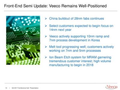
Veeco MRAM IBE slide, Q3-2017

Veeco says that its Ion Beam technology is well suited for etching the multilayer magnetic stack used in MRAM chips. Veeco already placed systems at multiple customers and expect high volume manufacturing to start next year for embedded memory applications.

Read the full story Posted: Nov 03,2017

Samsung will be ready with MRAM chips "soon"

Samsung's semiconductor chief Kim Ki-nam says that Samsung is developing next-generation memory technologies, such as MRAM and RRAM. According to Kim "Samsung will commercialize MRAMs and ReRAMs according to our own schedule. We are on our way and will be ready soon"

Samsung targets MRAM as an update to DRAM memory, while RRAM will be used as a storage memory to replace NAND.

Read the full story Posted: Apr 21,2016

New etching process developed specifically for MRAM production

Researcher from Cornell's NanoScale Science and Technology Facility (CNF), in collaboration with Oxford Instruments Plasma Technology (OIPT) developed a new etching process targeted specifically for MRAM device fabrication.

The MTJ developed by CNF and OIPD

The etching of the MTJ stack is a challenging step in MRAM fabrication, because the magnetic materials do not easily react to etching agents, and so manufactures usually use purely physical ion milling processes - which results in low etch rates, low selectivity and damage to the device structure itself.

Read the full story Posted: Mar 06,2016

Coughlin sees the MRAM market growing to over $1.3 billion in 2020

A new report from Coughlin Associates says that in the near future we will see dramatic changes in the memory market as as fast non-volatile memories augment and eventually replace volatile memory.

Memory technology shipping storage capacity forecast (Coughlin)

MRAM (and STT-MRAM) annual shipping capacity will rise from 240TB in 2014 to between 15 and 35 PB in 2020. MRAM and STT-RAM revenues are expected to increase from about $300 million in 2014 to between $1.35 and $3.15 billion by 2020.

Read the full story Posted: Nov 15,2015

Crocus raised $21 million, has over 250 sensor customers, will break even in Q1 2016

Crocus Technology has secured $21 million in a new financing round. All of Crocus' historical French and international investors participated in the round, including NanoDimension, Innovation Capital, IdInvest Partners, and Rusnano. Founded in 2004, Crocus has raised $194 million to date.

Crocus says that since it began producing MLU-based magnetic sensors in mid-2014, they have over 250 customers. The new capital will help Crocus to deploy its sensor product line in the key target markets: industrial, consumer electronics, automotive and solutions for IoT. Crocus will also strengthen its commercial resources (including finalizing a distribution network in Asia and reinforcing the support team) and develop develop new designs to enrich the product portfolio with integrated sensor and smart sensor applications. Crocus aims to reach breakeven in Q1 2016.

Read the full story Posted: Jun 19,2015

A leading edge semiconductor maker orders a full suite of STT-MRAM metrology tools from MicroSense

MicroSense announced that they installed a full suite of STT-MRAM magnetic metrology tools at a leading edge semiconductor manufacturer. These metrology systems characterize the magnetic properties of multi-layer 300 mm wafers or coupons used in the development and manufacturing of Perpendicular and In-Plane STT-MRAM.

The company says that this is the first time a major customer ordered a full suite of their tools to use in an STT-MRAM program. This order includes a Polar Kerr system for 200mm or 300mm Perpendicular STT-MRAM wafers and a KerrMapper tool for 200mm or 300mm In-plane STT-MRAM wafers. MicroSense's EZ Vibrating Sample Magnetometer measures sample coupons from Perpendicular or In-Plane STT-MRAM wafers.

Read the full story Posted: Jan 15,2014

ISI launches a Gen3 Pulser module for the WLA-3000STT-MRAM Analyzer

Integral Solutions International (ISI) announced a new module the WLA-3000 STT-MRAM Wafer Level Analyzer, the Gen3 Pulser. The new module is optimally matched with its proprietary probecard interface to produce programmable pulses as low as 5nS, with in-situ ability to perform ultra-fast measurements on the MTJs after pulsing.

The tester can be equipped with either the single or dual-channel pulse generator modules for improved UPH. The Gen3 Pulser module was redesigned to speed up Pulse related tests by an order of magnitude and features new Error Rate test (it can measure Error Rate of 10^6 in approximately 2 seconds). It is noew possible to characterize error rate as a function of VBias, Pulse Width/Amplitude, Field and other sweep parameters.

 
Read the full story Posted: Dec 14,2013

20 chipmakers from Japan and US to co-develop MRAM in hopes to replace DRAM within 3 years

According to Nikkei, over 20 Japanese and US companies have teamed up to develop MRAM technologies, in particular a new mass production method. Participants in this ambitious project include Tokyo Electron (who's merging with Applied Materials), Renasas, Hitachi and Shin-Etsu Chemical from Japan and Micron Technology from the US.

Japan's Tohoku University, a leader in Spintronics and MRAM research, will also join the project. The companies will finance several dozens researchers at the University. They plan to start development in February 2014, and continue to seek more companies from the US and Europe to join. The aim is to complete materials and processes development by 2017 and start mass production by 2018.

Read the full story Posted: Nov 24,2013

Jusung Engineering to supply MRAM etching and deposition equipment to Crocus's Russia fab

Jusung Engineering announced today that they will supply integrated etch and deposition system for Crocus Nanoelectronics (CNE)'s advanced OLED production. CNE is Crocus Technology's and RUSNANO joint-venture that aims to produce MRAM chips in Russia.

Jusung Engineering will supply the Genaon Plus MRAM etching equipment. this is a core process tool that can etch non-volatile materials such as platinum, manganese and cobalt. According to Jusung, this plasma etching equipment is specialized for magnetic metal layers patterning and it can completely eliminate polymer residue left behind on the side walls during the etching process.

Read the full story Posted: Sep 17,2013

Crocus licenses their MLU technology to TowerJazz, products expected by the end of 2013

Crocus Technology signed a license and joint-promotion agreement with TowerJazz, for the use of Crocus' Magnetic Logic Unit (MLU) process technology. TowerJazz customers will be able to use Crocus' technology in embedded System-On-Chip (SoC) applications. First products based on MLU are expected on the market before the end of 2013 as some customers are already in the process of adopting the technology.

Crocus's MLU blocks are used in magnetic sensors and secure embedded memories. The memory is fast (like DRAM) and non volatile. It also includes unique security options. Crocus actually plans to produce (at TowerJazz's Migdal Haemek manufacturing facility in Israel) their own magnetic sensor and non-volatile memory products.

Read the full story Posted: May 23,2013