MRAM Manufacture

MRAM Manufacture, equipment, process, etc.

Hprobe and NY CREATES to co-develop next-generation MRAM testing capabilities

Hprobe, a developer of testing equipment for magnetic devices, announced a strategic collaboration with NY CREATES, a lab-to-fab bridge for advanced electronics, to advance testing capabilities for next-generation semiconductor memory technologies. This joint development project will focus on the co-development of advanced testing equipment at the 300mm wafer scale.
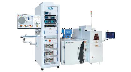
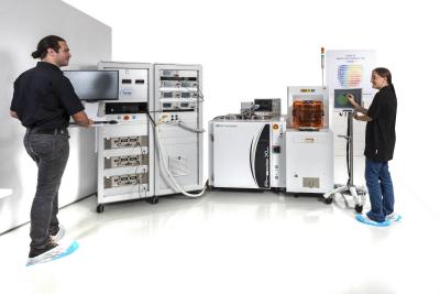
Hprobe IBEX WAT H3DM Light photo

NY CREATES and Hprobe will work together to support new testing solutions for MRAM, RRAM and selector devices. The joint project will focus on initial testing of MRAM and RRAM wafers from NY CREATES using Hprobe’s equipment, including the full-scale implementation of Hprobe’s IBEX wafer-level magnetic tester. Development of breakthrough testing procedures and algorithms for MRAM, RRAM, and selector devices, will also seek to advance the state-of-the-art in semiconductor memory testing.

Read the full story Posted: Nov 13,2024 - 1 comment

Hprobe releases a new MRAM testing module to help increase production yields

Hprobe, a developer of testing equipment for magnetic devices, announced a new addition to its product line, the RF Pulse Module. The company says that this is the commercially available testing system to both collect statistics of error rate of the memory unit cell and take a deep look into switching dynamics of resistive memories.

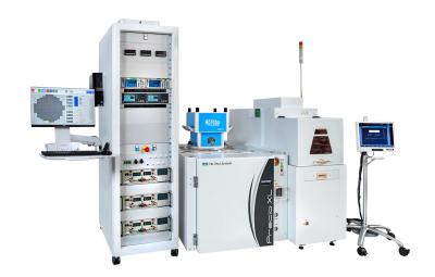
Hprobe IBEX WAT H3DM Light photo

Hprobe's IBEX system

Hprobe says that the RF Pulse Module is two orders of magnitude faster than existing devices and can help increase manufacturing yields. Hprobe has already begun shipping to tier-1 companies and major research institutes around the world.

Read the full story Posted: Dec 03,2022

ISI introduces a new 3-Axis magnet option for its MRAM tester systems, targeting STT-MRAM and SOT-MRAM testing

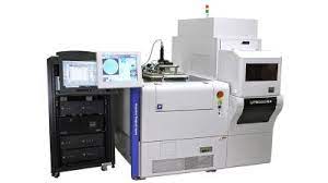
Integral Solutions International (ISI) announced a new 3-Axis Magnet Option for wafer-level testing. Combined with ISI's WLA5000 Tester, the 3D magnetic fields produced by this system can be used for characterization of MRAM devices in addition to 2D/3D Magnetic Sensors.

ISI WLA5000 MRAM tester

ISI says that for MRAM applications, the 3D Magnetic fields produced by ISI’s 3-Axis Magnet Option delivers solutions for both STT-MRAM and SOT-MRAM applications.

Read the full story Posted: Mar 04,2022

Hprobe announces a large magnetic tester order from a Korean semiconductor maker

Hprobe, a developer of testing equipment for magnetic devices, announced a significant order from a tier-1 semiconductor manufacturer in Korea for a wafer-level magnetic tester.

Hprobe IBEX WAT H3DM Light photo

Hprobe's IBEX platform is compatible with 200mm and 300mm automated wafer probers, and is dedicated to testing MRAM magnetic tunnel junctions, bit cells based on STT-MRAM, SOT-MRAM, and Voltage Controlled (VC-MRAM) technologies.

Read the full story Posted: Feb 04,2022

Hprobe announces a significant order for MRAM testing equipment from a tier-1 semiconductor manfacturor

Hprobe, a developer of testing equipment for magnetic devices, announced a 'significant' order for a wafer-level magnetic tester (the company's IBEX tester) from a tier-1 semiconductor manufacturer.

The equipment will be used for research and development of magnetic materials and devices, which represents a very promising technology for MRAM chips and magnetic sensors. The IBEX platform is compatible with 200mm and 300mm automated wafer probers, and is dedicated to testing MRAM magnetic tunnel junctions, bit cells based on STT-MRAM, SOT-MRAM, and Voltage Controlled (VC-MRAM) technologies.

Read the full story Posted: Apr 28,2021

Successful MRAM Production Requires Good Magnetic Test Equipment

This is a sponsored post by Integral Solutions Int'l

MRAM is likely to be the most promising next-generation non-volatile memory technology today. Toggle MRAM and STT-MRAM are already entering the market, gaining market share in many applications. Next-generation MRAM technologies, such as SOT-MRAM could enable the replacement of even the fastest SRAM applications, with higher densities.

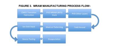
MRAM Manufacturing Process Flow (Coughlin)Source: Coughlin Associates, 2019

The MRAM production process has many stages, as device architecture is relatively complex, with a magnetic cell (frontplane) fabricated on top of a CMOS backplane. (use Figure 2 or Figure 3 from Coughlin). Measurement and characterization of devices are highly important, and the production of MRAM memories depend on measurement tools are are specialized for MRAM and STT-MRAM measurements.

Read the full story Posted: May 26,2020

Hprobe raises over 2 million Euros to support its MRAM device testing equipment development

Hprobe, a developer of testing equipment for magnetic devices, has raised more than 2 million euros from a group of international investors. The new funds will support Hprobe's spintronics device testing development - which include MRAM and TMR sensors.

Hprobe MRAM Wafer Level Magnetic Tester on a TEL Prober photo

The investment round was led by Germany-based High-Tech Gründerfonds (HTGF), a public-private venture capital investment firm. Other investors include Taiwan ITRI's ITIC VC firm and TEL Venture Capital.

Read the full story Posted: Feb 06,2020

Applied Materials unveils new high-volume 300mm MRAM manufacturing system

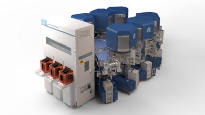
Applied Materials unveiled new high-volume manufacturing solutions for next-generation memories. The Endura platform integrates multiple materials engineering technologies along with on-board metrology to create new films and structures.

Applied Materials Endura Clover MRAM PVD system photo

Applied’s new Endura Clover MRAM PVD platform is made up of nine unique wafer processing chambers all integrated in pristine, high-vacuum conditions. Applied says that this is the industry's first 300-millimeter MRAM system for high-volume manufacturing capable of individually depositing up to five different materials per chamber. The Clover MRAM PVD platform includes on-board metrology that measures and monitors the thickness of the MRAM layers with sub-angstrom sensitivity as they are created to ensure atomic-level uniformity.

Read the full story Posted: Jul 12,2019

Analysts expect MRAM revenues to grow 170X by 2029 to reach $4 billion

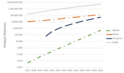
A new market report by Objective Analysis and Coughlin Associates expects that stand-alone MRAM and STT-MRAM revenues will grow 170X from 2018 to 2029, reaching almost $4 billion in revenues. The growth of next-generation memory technologies will be mainly driven by displacing today’s less efficient memory technologies like NOR flash and SRAM.

MRAM capacity shipments forecast (2017-2029, Coughlin)The analysts expect many memory technologies, including DRAM, 3D Xpoint and NAND to grow in the coming years, but the most stellar growth will be of MRAM memories. Shipments in terms of capacity are expected to grow from around 0.1 Petabytes in 2019 to almost 1 million Petabytes by 2029.

Read the full story Posted: Jul 09,2019

Keysight Technology announces a new MRAM test platform designed in collaboration with Tohoku University

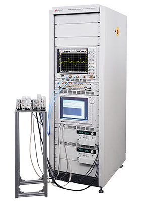
Tohoku University's Center for Innovative Integrated Electronic System (CIES) announced that its collaboration with Keysight Technology has led to the release of a new MRAM test platform product, the NX5730A.

Kesight NX5730A Memory Test system photo

Keysight's NX5730A is a high-throughput 1 ns Pulsed IV memory test solution. Keysight says that this solution is a unique dedicated system for characterizing emerging devices such as magnetic tunnel junction (MTJ) on silicon wafers, accelerating the efficiency of device characterization and memory production testing.

Read the full story Posted: Nov 08,2017