![]() IBM develops and supplies computer hardware, software, services and research. IBM says has produced more research breakthroughs than any other company in the IT industry.
IBM develops and supplies computer hardware, software, services and research. IBM says has produced more research breakthroughs than any other company in the IT industry.
IBM is an MRAM pioneer, collaborating with both Infineon and Samsung. In 2016, IBM and Samsung researchers demonstrated 11 nano-meter STT-MRAM junctions. In 2020, the company unveiled the first 20 nm STT-MRAM node.
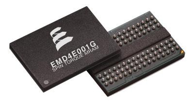
IBM also uses MRAM memory in some of its products. In 2024 Everspin announced that IBM has chosen the PERSYST EMD4E001G 1Gb STT-MRAM for use in their FlashCore Module 4.
1 New Orchard Road
Armonk, NY 10504-1722
United States
IBM's next-gen FlashCore modules to feature Everspin's 1 Gbg STT-MRAM
Everspin announced that IBM has chosen the PERSYST EMD4E001G 1Gb STT-MRAM for use in their FlashCore Module 4.

Everspin says that its EMD4E001G high-performance persistent memory ensures critical data integrity even during power loss. With a DDR4 interface, it delivers 2.7 gigabytes/second of both read and write bandwidth, coupled with instant non-volatility.
IBM to reveal the world's first 14nm STT-MRAM node
IBM announced that during the 2020 IEEE International Electron Devices Meeting (IEDM 2020), that is now being held virtually, its researchers will reveal the first 14 nm node STT-MRAM. IBM says that efficient and high-performance STT-MRAM systems will help to address memory-compute bottlenecks in hybrid cloud systems.
IBM says that the 14 nm node embedded MRAM which will be revealed is the most advanced MRAM demonstrated to date. It features circuit design and process technology that could soon enable system designers to replace SRAM with twice the amount of MRAM in last-level CPU cache.
IBM to use Everspin's 1Gb STT-MRAM in its next-gen FlashCore modules
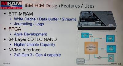
In August 2018 IBM announced that it adopted Everspin's 256Mb STT-MRAM chips in its enterprise SSD FlashSystem. Now IBM announced that it's latest FlashCore modules will use Everspins 1Gb STT-MRAM chips.

Using MRAM instead of DRAM memory enabled IBM to remove the relatively large supercapacitors (used to make the DRAM non-volatile) and so the company was able to reduced the size of its drives and switch to a standard 2.5-inch U.2 drive form factor.
IBM introduces its latest 19.2TB enterprise SSD drivers with Everspin's STT-MRAM
A couple of days ago, Everdisplay disclosed its first major design win with a "top enterprise storage vendor" for its 40nm 256Mb STT-MRAM chips. We now know that this vendor is IBM - as it introduced its latest-generation enterprise SSD FlashSystem, which indeed includes Everspin's STT-MRAM.

Using MRAM instead of DRAM memory enabled IBM to remove the relatively large supercapacitors (used to make the DRAM non-volatile) and so the company was able to reduced the size of its drives and switch to a standard 2.5-inch U.2 drive form factor. The new FlashSystem SSDs support up to 19.2TB of 64L 3D TLC NAND. IBM's system uses a 20-channel NAND interface and a four-lane PCIe 4.0 host interface that can operate in dual-port 2+2 mode.
Interview with Bo Hansen, CEO at Capres A/S
 Capres A/S was established in 1999 in Denmark to develop a unique probe technology designed for in-line production monitoring in the semiconductor industry. The company, in collaboration with IBM, developed a resistivity measurement technique to characterize MTJ stacks.
Bo Svarrer Hansen, the company's CEO since 2002, was kind enough to answers a few questions we had, and share with us his views on the MRAM market and the company's measurement systems for MRAM and STT-MRAM device developers.
Q: Can you update us on Capres' current offers to the MRAM industry?
Capres customers are using our CIPTech® tools for R&D on small samples as well as volume production on 300 mm wafers. Depending on the configuration the tools measure with an in- plane or an out- of- plane magnetic field on blanket as well as patterned wafers.
IBM demonstrated 11nm STT-MRAM junction, says "time for STT-MRAM is now"
IBM researchers, in collaboration with Samsung researchers, demonstrated switching MRAM cells for devices with diameters ranging from 50 down to 11 nanometers in only 10 nanoseconds, using only 7.5 microamperes. The researchers say that this is a significant achievement on the way to high-density low-power STT-MRAM.

Using perpendicular magnetic anisotropy (PMA), the researchers can deliver good STT-MRAM performance down to 7×10⁻¹⁰ write-error-rate with 10 nanosecond pulses using switching currents of only 7.5 microampere.
IBM demonstrates Everspin's ST-MRAM in its ConTutto platform in a Power8 system
Everspin announced that IBM has demonstrated the company's Spin Torque DDR3 MRAM in the ConTutto platform in a Power8 system. IBM showed show how Everspinâs ST-MRAM operates as persistent memory, accelerating storage and server applications.

ConTutto is an IBM research configurable platform for innovation in the memory subsystem of an OpenPOWER node. The DDR3 interface on the Everspin Spin Torque MRAM makes it easy for developers to take advantage of the write speed and persistence of MRAM.
Crocus raised $45 million, hopes to start generating revenue towards the end of 2013
 Crocus Technology have completed their Series D round of funding, raising â¬34 million (about $45 million). The company raised $80 so far (not counting the $300 million from RUSNANO towards a manufacturing fab in Russia). The company hopes to start generating revenue by the end of 2013 and become cashflow break-even by the end of 2014.
Crocus are rather busy. They will use the money to ramp up its manufacturing at Tower Semiconductors (in Israel) while also qualifying its Russian joint venture fab in Moscow. They expect first engineering wafers in the summer.
Crocus and IBM to jointly-develop MRAM technology, sign patent license agreements
Crocus signed a joint technology development agreement and a mutual patent license agreement with IBM. They also signed a technology agreement - under which they will jointly develop semiconductor technology that combines Crocus' thermally assisted next generation Magnetic-Logic-Unit (MLU) technology with IBM's MRAM technology and processing capabilities.
MLU is a scalable evolution of Crocus' Thermally Assisted Switching (TAS) technology, and enables practical implementation of advanced magnetic logic and memory capabilities.
IBM report advances in racetrack memory research
 IBM reports some advances in their racetrack memory program, and they are now able to measure the movement and processing of data as a magnetic pattern on a nanowire (which is 1,000 finer than a human hair).
Racetrack memory uses electron spin to move data on nanowires at hundreds of miles per hour... IBM is not commercializing it yet, but racetrack memory has the potential to be very lower-power and high-density.
Pagination
- Page 1
- Next page


