STT-MRAM - Page 10

IMEC researchers demonstrate the world's smallest pMTJ at 8nm

Researchers at IMEC developed a 8nm perpendicular magnetic tunnel junction (pMTJ) with 100% tunnel magnetoresistance (TMR) and a magnetic coercive field up to 1,500 Oe in strength. The researchers also demonstrated integrated 1Mbit STT-MRAM 1T1MTJ arrays with pitches down to 100 nm.

IMEC says that this is the world's smallest pMTJ - which paves the way for high density stand-alone MRAM applications. The pMTJ was developed on 300mm silicon wafers in a production process that is compatible with the thermal budget of standard CMOS back-end-of-line technology.

Read the full story Posted: Dec 07,2016

The EU-funded GREAT project presents its first hybrid CMOS-MRAM 180nm tape out

GREAT Project logoIn 2015, the EU launched the GREAT project, with an aim to co-integrate multiple functions like sensors, RF receivers and logic/memory together within CMOS by adapting STT-MTJs to a single baseline technology in the same system on chip. GREAT stands for heteroGeneous integRated magnetic tEchnology using multifonctionnal stAndardized sTack.

The project partners now announced the first hybrid CMOS/MSS-MRAM Tape Out with Israel-based Tower Jazz. This hybrid integrated circuit uses the 180nm CMOS process from Tower and an academic MRAM post-process that will be done by CEA Spintec within their facilities.

Read the full story Posted: Nov 20,2016

Interview with Bo Hansen, CEO at Capres A/S

Bo Hansen, Capres CEOCapres A/S was established in 1999 in Denmark to develop a unique probe technology designed for in-line production monitoring in the semiconductor industry. The company, in collaboration with IBM, developed a resistivity measurement technique to characterize MTJ stacks.

Bo Svarrer Hansen, the company's CEO since 2002, was kind enough to answers a few questions we had, and share with us his views on the MRAM market and the company's measurement systems for MRAM and STT-MRAM device developers.

Q: Can you update us on Capres' current offers to the MRAM industry?

Capres customers are using our CIPTech® tools for R&D on small samples as well as volume production on 300 mm wafers. Depending on the configuration the tools measure with an in- plane or an out- of- plane magnetic field on blanket as well as patterned wafers.

Read the full story Posted: Oct 26,2016

Avalanche to commence volume pMTJ STT-MRAM production in early 2017

STT-MRAM developer Avalanche Technology announced that volume production of its pMTJ STT-MRAM chips on 300 mm wafers will begin in early 2017. Avalanche started to sample 32Mb and 64Mb STT-MRAM chips in 2015

Avalanche has entered into a manufacturing agreement with Sony Semiconductor Manufacturing Corporation (SSMC) for this volume production. Avalanche targets several markets, including Storage, Automotive, IoT and embedded applications. Avalanche will offer discrete MRAM chips from 4Mb to 64Mb in size.

Read the full story Posted: Oct 21,2016

Spin Transfer Technologies fabricated 20nm OST-MRAM MTJs, preparing to deliver samples

Spin Transfer Technologies (STT) announced that it fabricated 20nm perpendicular MRAM magnetic tunnel junctions (MTJs) based on the company's Orthogonal Spin Transfer MRAM (OST-MRAM).

STT is now preparting to deliver OST-MRAM samples to select customer, following requests from "certain major semiconductor and systems companies". The company is processing more than 40 wafer lots at its R&D fab in Fremont, California.

Read the full story Posted: Sep 27,2016

Samsung Foundry to start offering STT-MRAM by 2019

Back in July 2016 (yes, we missed that one, but better late than never), Samsung Foundry's business development chief Kelvin Low said that the company is set to offer STT-MRAM on its 28nm FDSOI manufacturing process by the end of 2018.

To be more precise, the STT-MRAM in 2018 will be on a not-finalized process (what Samsung calls Risk Production Phase) - and real volume production will only begin in 2019. Samsung will be pushing its eFlash 28nm production before STT-MRAM will be available - but the company expects MRAM to be a favorite in the long term.

Read the full story Posted: Sep 23,2016

Everspin to demonstrate the world's fastest SSD based on its ST-MRAM

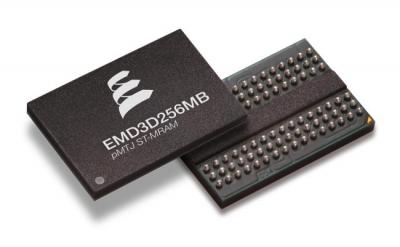
Everspin announces that it is going to demonstrate the world's fastest solid-state drive (SSD) using its latest perpendicular ST-MRAM technology. The drive achieves continuous write operations of 1.5 Million IOPS, using Everspin's Everspin’s 256Mb DDR3 chips (manufactured by global foundries).

Everspin started sampling its new pMTJ ST-MRAM chips last month. The p-MTJ ST-MRAM offers improved performance, higher endurance, lower power, and better scalability compared to previous MRAM and ST-MRAM products. Everspin is developing on a scaled-down 1Gb version.

Read the full story Posted: Sep 11,2016

Aupera Technologies launches the world's first storage module based on Everspin's pMTJ STT-MRAM

Aupera Technologies launched the world's first M.2 storage module based on Everspin's recently announced 256Mb pMTJ ST-MRAM. The Aup-AXL-M128, will be used in Aupera's All Flash Array system as a hardware acceleration engine for specific applications that require low latency and high performance.

Aupera Aup-AXL-M128 photo

Aupera says the company is excited at the future potential of this ST-MRAM based module. The ST-MRAM delivers four orders of magnitude BER reduction and more than 30% less power while quadrupling the capacity to 128MB as compared to the previous generation M.2 MRAM module.

Read the full story Posted: Aug 10,2016