STT-MRAM - Page 17

A*STAR patents low-density parity-check (LDPC) coding with soft decision decoding for STT-MRAM devices

A*STAR scientists have filed a patent on low-density parity-check (LDPC) coding with soft decision decoding. This is an advanced error correction coding scheme STT-MRAM devices. Hopefully this new scheme will enable more relaxed smaler STT-MRAM designs that can rely on the error-correction.

STT-MRAM devices suffer from cell errors due to imperfections in the fabrication process (variation in the tunneling oxide thickness and cross-section area). The researchers explain that conventional (hard decision) error correction codes do not work very well on STT-MRAM cells. The new soft decision decoding works on the probability of each detected bit as being a 0 or 1 (i.e. soft reliability), and hence has less decoding errors than the conventional hard decision decoding.

Read the full story Posted: Mar 15,2012

Spin Transfer Technologies raised $36 million to accelerate its OST-MRAM technology development

Spin Transfer Technologies (STT) announced that they raised $36 million in series A funding led by parent company, Allied Minds and Invesco Asset Management. STT will use the money to accelerate the development of its patented orthogonal spin transfer magneto resistive random access memory technology (OST-MRAM) - by scaling operation, hiring new employees and purchasing equipment.

This is great news for STT. The last we heard from the company was in November 2010 when they announced the successful development of the STT-MRAM device that uses STT's proprietary orthogonal spin transfer technology with a magnetic tunnel junction (MTJ) for memory state read-out.

Read the full story Posted: Feb 14,2012

Interview with Barry Hoberman, Crocus' chief marketing officer

Crocus is a startup company that develops MRAM technology - and recently they have announced several exciting advances in both their technology and their financing and production plans. We had the good chance to interview Barry Hoberman, Crocus' chief marketing officer.

Q: Barry, thanks for agreeing to answer our questions... The big story today is still RUSNANO's $125 million investment - announced in May 2011. Any updates on this deal? Have the construction begun on the Russian plant?

A: The site selection for our Russian plant (Crocus Nano Electronics) has been completed. The site contains an existing shell, which will be modified to support the clean room. Crocus expects to process wafers at this facility in 2013.

Read the full story Posted: Jan 08,2012

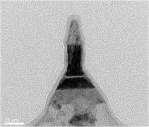
Samsung developed a perpendicular MTJ at 17nm

Samsung developed a perpendicular MTJ element using 17nm technology - the world's smallest. This paves the way towards sub-20nm STT-MRAM. Up until now it was believed that to create such a small P-MTJ you will have to use a multi-layer structure and a rare-earth material for the ferromagnetic electrode. Samsung however used regular materials and structure (Ta/CoFeB/MgO/Ta) and optimized the oxidation process for the tunnel insulator (MgO).

By increasing the anisotropic energy on the joint interface the perpendicular magnetization of the ferromagnetic electrode was stabilized. Samsung reports a thermal stability factor of 34, a TMR ratio of 70% and a writing current of 44microampere with a perpendicular magnetization MTJ element whose cross-section area is 17 x 40nm. There is still room for improvement in the thermal stability factor in order to achieve over 1Gbit capacity at 20nm. This can be realized by making more improvements to the newly developed oxidation process for the tunnel insulator

Read the full story Posted: Dec 11,2011

Toshiba designed an STT-MRAM/SRAM hybrid cache for ultra-low power processors

Toshiba has a new hybrid cache design that uses STT-MRAM and SRAM combination. This is aimed towards next-generation low-power computer processors. These new computers will usually be off, and the time and power it takes to "wake up" is considerable. The new design can reduce the energy consumption by around half - and does not effect processing capacity.

Toshiba's design uses a 512Kb STT-MRAM cache combined with a 32Kb register file and a 64Kb SRAM primary cache. Using the non-volatile MRAM, the power gating can be conducted more frequently. In current designs, it takes around 20 micro seconds to recover from power gating and about 150 micro seconds from deep-sleep mode. In the new design, it takes only 1 micro second to recover from power gating.

Read the full story Posted: Nov 08,2011

Micron and A*STAR to jointly develop high density STT-MRAM

Micron and the A*STAR Data Storage Institute (DSI) from Singapore announced that they will jointly develop STT-RAM. The two companies will invest in a 3-year joint-research program to develop high-density STT-MRAM devices.

Years ago Micron had an active MRAM program which was scrapped in October 2004. It's great to see them re-enter MRAM research. Scott DeBoer, Micron Vice President of Research and Development said that Micron is "actively working on multiple emerging memory development programs" - and this collaboration is seen as a way to "explore the potential of STT-MRAM"

Read the full story Posted: Oct 29,2011

Everspin to launch STT-MRAM in 2012, partners with Cadence on memory models

Everspin is gearing up to introduce their upcoming STT-MRAM products in 2012, and the company announced that they have partnered with Cadence to provide ;memory model verification IP for these products. The new memory models are already available as part of the Cadence Verification IP Catalog. Everspin says they are working with several partners to ensure design-in tools are available as well.

STT-MRAM requires less current to write info into the memory cell, which leads to higher densities. Everspin's current highest-density Toggle-MRAM product is a 16Mb chip, and we expect their STT-MRAM products to be much higher in density, which will open new markets and applications.

Read the full story Posted: Oct 04,2011

Samsung acquires Grandis

Samsung announced that it has acquired Grandis, developer of STT-MRAM technology. We do not have any financial details yet, but Grandis' CEO Frahad Tabrizi said that this deal serves as a& "very successful exit" for Grandis's investors. Grandis raised $15 million since it was founded in 2002 (and also raised about the same from DARPA grants including a $8.6 million second-phase project granted in June 2010).

Grandis licensed their technology to several companies. We know that Hynix licensed it in 2008. The company was also collaborating with Renesas technologies. Hynix and Grandis were developing a compact in-plane MTJ based STT-RAM device that uses modified DRAM processes at 54nm.

Read the full story Posted: Aug 02,2011

Toshiba and Hynix to co-develop and produce MRAM products

Toshiba and Hynix announced an agreement to jointly develop MRAM products. Once the development is complete, the companies intend to establish an MRAM production plant together. We believe the companies intend to develop STT-MRAM technology.

Toshiba has been developing STT-MRAM for quite some time, and just a few days ago reported a breakthrough MTJ device that could pave the way towards Gigabit MRAM devices. They expect such chips within 3-4 years, so that's probably the same time frame on the new JV with Hynix.

Read the full story Posted: Jul 13,2011

Toshiba report STT-MRAM advances, expects gigabit chips within 3-4 years, to be cost competitive to DRAM

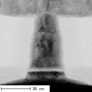
Toshiba says that their newly developed perpendicular magnetization-type magnetic tunnel junction (MTJ) device has excellent properties - and it can be a basic element towards a gigabit STT-MRAM device. The company says that these 'research results' are encouraging and they will now shift to the development of products. Commercialization of gigabit STT-MRAM is expected within 3 to 4 years.

MTJ cross section (Toshiba)MTJ cross section (Toshiba)

The device's writing current density is 5 x 10⁵Acm-2, which is 1/6 that of the company's existing products. And its magnetic resistance (MR), which determines data reading margin, is 200%, which was drastically improved from the 15% of the existing products. Toshiba managed to have both a low writing current density and a high MR ratio by using cobalt and iron based materials for the recording layer.

Read the full story Posted: Jul 06,2011