pMTJ - Page 4

Spin Transfer Technologies produced working 60-nm STT-MRAM prototypes

Spin Transfer Technologies (STT) has successfully produced a working prototype STT-MRAM device. The company's advanced prototyping magnetics processing line at its facility in Fremont, California, is now fully operational.

STT's prototypes incorporate proprietary, performance-enhancing ‘spin-filtering’ technology, and were fabricated on industry standard CMOS wafers sourced from a high volume Asian foundry supplier. The prototypes are based on 60-nm perpendicular magnetic tunnel junction devices

Read the full story Posted: Feb 04,2016

STT-MRAM maker Avalanche Technology raised $23 million

STT-MRAM developer Avalanche Technology raised $23 million from Thomvest Ventures, Vulcan Capital, Rogers Venture Partners, and VTB Capital. The company also has a substantial debt facility in place with Horizon Technology Finance.

Avalanche say that they are now bringing their Spin-Programmable STT-MRAM (SPMEM) discrete products to Tier-1 OEMS and licensing their embedded solutions (AvRAM) to strategic partners. The company previous financing round was announced in July 2012.

Read the full story Posted: Feb 03,2016

Avalanche Technology starts to sample 32/64 Mbit STT-MRAM chips

STT-MRAM developer Avalanche Technology announced that it began to sample STT-MRAM chips. Avalanche's proprietary perpendicular magnetic tunnel junction (pMTJ) cells are manufactured in a high volume, low cost, standard CMOS 300mm process.

Those first sample chips are 32Mbit and 64Mbit in size, and offer an industry-standard SPI interface built on a 55nm-node foundry process. Avalanche is also offering its STT-MRAM technology (which they brand as AvRAM) under license as embedded memory for integrated SOC designs.

Read the full story Posted: Jul 03,2015

Toshiba shows a new STT-MRAM test chip that consumes about 80% less power than SRAM memory

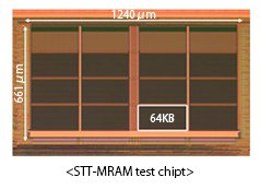
Toshiba presented a new STT-MRAM 1-Mb test chip that provides speed performance capable of 3.3-ns access to in-cache memory. The newly developed circuit consumes about 80% less power compared to a conventional SRAM as embedded memory - and Toshiba says that this makes it the best power-performing embedded memory.

Toshiba STT-MRAM test chip (Feb 2015)

To make this chip, Toshiba developed a new class of magnetic materials, that enabled them to build this low-power, high-efficiency, high-speed performance in energy-efficient magnetic tunnel junction (MTJ) memory.

Read the full story Posted: Mar 07,2015

Avalanche Technology announce four additional key MRAM and STT-MRAM patents

Avalanche Technology has been awarded new key patents in the areas of STT-MRAM technology, MRAM integration and manufacturing and perpendicular Magnetic Tunnel Junction (pMTJ) STT-MRAM. This follows eight new key patents awarded to Avalanche since the beginning of 2014.

Avalanche (founded in 2006 and based in California, US) developed patented Spin Programmable STT-MRAM (SPMEM) memory that uses a revolutionary proprietary spin current and voltage switching technology. The company wants to license their technology for embedded applications and also build discrete standalone memory devices. In July 2012 the company raised $30 million.

Read the full story Posted: Aug 08,2014

Toshiba developed STT-MRAM based microprocessor cache memory

Toshiba developed new STT-MRAM technology that can be used to enable MRAM based cache memory for microprocessors. The L2 cache alone uses about 80% of the power consumed by the CPU, so reducing the power consumption of the cache is very important - and STT-MRAM may reduce this consumption by about 60%. It's not clear how close is this technology to actually being commercialized.

Toshiba's new STT-MRAM uses a dual-cell (2T-2MTJ) circuit in which the two MTJs have complementary resistive states (high and low resistive states). This eliminates the leak path and also increases the readout signal intensity - and so improves access speed. In Toshiba's cahce, the read time is 4.1 ns - very close to that of SRAM, while the write time (2.1ns) is similar to SRAM. Toshiba also implemented error correction mechanisms into the cache STT-MRAM chip.

Read the full story Posted: Jun 12,2014

Avalanche has been awarded four more key STT-MRAM patents

Last month we reported that Avalanche Technology has been awarded four key "milestone" patents for its STT-MRAM technology and solid-state storage array system design. Today the company announced that it has been awarded four new STT-MRAM patents in areas of Perpendicular STT-MRAM and MRAM Integration and Manufacturing. Avalanche has over 200 filed patents that covers the full spectrum from memory cell/circuit design and manufacturing to solid-state storage system development and deployment.

The company has been awarded three key patents in the area of Perpendicular STT-MRAM:

Read the full story Posted: Apr 22,2014

Avalanche has been awarded four key "milestone" STT-MRAM patents

Avalanche Technology has been awarded four key "milestone" patents for its STT-MRAM technology and solid-state storage array system design. Avalanche has over 200 filed patents that covers the full spectrum from memory cell/circuit design and manufacturing to solid-state storage system development and deployment.

Avalanche (founded in 2006 and based in California, US) developed patented Spin Programmable STT-MRAM (SPMEM) memory that uses a revolutionary proprietary spin current and voltage switching technology. The company wants to license their technology for embedded applications and also build discrete standalone memory devices. In July 2012 the company raised $30 million.

Read the full story Posted: Mar 26,2014

A leading edge semiconductor maker orders a full suite of STT-MRAM metrology tools from MicroSense

MicroSense announced that they installed a full suite of STT-MRAM magnetic metrology tools at a leading edge semiconductor manufacturer. These metrology systems characterize the magnetic properties of multi-layer 300 mm wafers or coupons used in the development and manufacturing of Perpendicular and In-Plane STT-MRAM.

The company says that this is the first time a major customer ordered a full suite of their tools to use in an STT-MRAM program. This order includes a Polar Kerr system for 200mm or 300mm Perpendicular STT-MRAM wafers and a KerrMapper tool for 200mm or 300mm In-plane STT-MRAM wafers. MicroSense's EZ Vibrating Sample Magnetometer measures sample coupons from Perpendicular or In-Plane STT-MRAM wafers.

Read the full story Posted: Jan 15,2014

Toshiba's new STT-MRAM based computing architecture to enable drastically faster and more efficient CPUs

Toshiba announced a new computing architecture that uses only STT-MRAM to perform both operations and storage. The idea support computing capability, register file, primary cache and secondary cache all on the same perpendicular STT-MRAM, and Toshiba says it could lead to CPUs that are drastically faster and more efficient.

Toshiba explains that in the new architecture, the results of operations (answers) that correspond to combinations of certain inputs are prepared in advance in the form of a table and stored in the memory. In response to an input, an answer is read out of the memory. This is equivalent to an operation carried out by a CPU. Because the computation answer is read once, it drastically improves processing speed and power consumption.

Read the full story Posted: Dec 12,2013