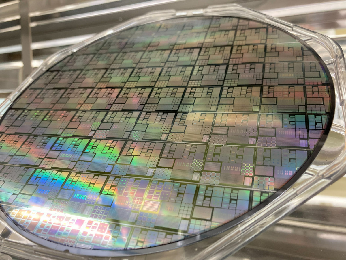
In 2022, Taiwan's Industrial Technology Research Institute (ITRI) announced an agreement with Taiwan Semiconductor Manufacturing Company (TSMC) to collaborate on SOT-MRAM R&D. ITRI and TSMC now announced that they have developed SOT-MRAM array chips that boasts a power consumption of merely one percent of a comparable STT-MRAM device.
ITRI and TSMC published a new research paper that was presented at the 2023 IEE International Electron Devices Meeting (IEDM 2023). ITRI explains that the new unit cell achieves simultaneous low power consumption and high-speed operation, reaching speeds as rapid as 10 nanoseconds. And its overall computing performance can be further enhanced when integrated with computing in memory circuit design.
ITRI is very active in MRAM research. In 2022, it also announced a collaboration with NYCU, to develop high-efficiency MRAM operating technologym. ITRI also announced a joint project with UCLA to develop VC-MRAM technologies.
TSMC has also been engaged with MRAM R&D and production for many years. In 2021, it presented its eMRAM roadmap. Last year TSMC announced a collaboration with NXP Semiconductors to offer automotive embedded MRAM, in TSMC's 16 nm FinFET technology. According to NXP, bringing together NXP’s high-performance S32 automotive processors with fast and highly reliable next-generation MRAM in 16 nm FinFET technology provides the ideal hardware platform for this transition.
In SOT-MRAM, or spin-orbit torque MRAM, the switching of the free magnetic layer is done by injecting an in-plane current in an adjacent SOT layer, unlike STT-MRAM where the current is injected perpendicularly into the magnetic tunnel junction and the read and write operation is performed through the same path. SOT-MRAM promises to be faster, denser and more efficient.


Comments
Relevant information about MRAM
As possible, when it is a news about Non Volatile Memory (NVM) MRAM, would it possible to also provide the information below (indicate unknown if the information wasn’t provided) and as possible to benchmark those information compared to STT-MRAM and DRAM and/or SRAM L3 cache :
1. read/write speed (ex: 1ns read and 10ns write)
2. power consumption for read and write (ex: 10 femtojoules/bit for read and 100 femtojoules/bit for write)
3. read/write reliability (10E12, or 10E14, or 10E16 ?)
4. retention time (at least 10 years, at least 20 years,…)
5. What are the shortcomings and area that still need to be improved to make it a possible candidate to transfer the technology in High Volume Manufacturing (HVM)
This would allow to immediately benchmark the results of the research and see the improvements made, and then see if the said MRAM would be better suited for DRAM replacement, or if it is fast enough to be considered for SRAM L3 cache or better…